(2) Well Formation
1.

=> n-well Mask
1) Photolithography
- HMDS
- PR coating
- Soft Bake
- Align and exposure
- PEB
- Develop
- Hard nake
2) Ion implantation
- Phosphorus, 120keV, 6x10^12cm^-2
3) PR strip
- Oxygen plasma ashing
- H2SO4 strip
2.
=> p-well Mask
1) Photolithography
- HMDS
- PR coating
- Soft Bake
- Align and exposure
- PEB
- Develop
- Hard nake
2) Ion implantation
- Boron, 80keV, 6x10^12cm^-2
3) PR strip
- Oxygen plasma ashing
- H2SO4 strip
3.

1) Pre-furnace cleaning
- SPM, SC1, SC2
- 고온 열처리하기 전에 시행
(∵ clenaing을 진행하지 않으면, 여러 오염 물질들이 확산 가능 -> 전기적 특성에 영향)
2) Well drive-in
- 1000도, 10h
- 목적) dopant diffusion 발생
3) SiO2 strip
4) Pre-furnace cleaning
- SPM, SC1, SC2
5) Buffer oxide re-grow
- thermal oxidation
- 목적) channeling 방지
(2-1) Threshold Voltage Adjustment
=> Vt가 낮을 때, channel 쪽에 doping을 하는 과정
=> pvt Mask
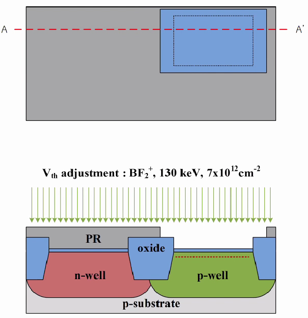
=> nvt mask
1) Photolithography
2) Ion implantation
3) PR strip
'반도체 공정' 카테고리의 다른 글
| CMOS process flow_LDD implantation/HDD implantation (0) | 2024.05.23 |
|---|---|
| CMOS process flow_gate stack deposition and patterning (0) | 2024.05.22 |
| CMOS process flow_isolation (0) | 2024.05.19 |
| CMOS Process Flow (0) | 2024.05.18 |
| Cleaning (0) | 2024.03.25 |


